|
MEMS technology
- 3D Stacked Die Create Unique Test Issues
- Instead, they will be attached with a through-silicon via (TSV) or in another way, and there may not be big enough probe pads to probe them during wafer ...
today Chip Design Magazine (blog) - MEMS technology
- I-Micronews - MEMS EQUIPMENT: Tegal expands ProNova(TM) ICP ...
- The Company's plasma etch and deposition tools enable sophisticated manufacturing techniques, such as 3D interconnect structures formed by intricate silicon etch, also known as Deep Reactive Ion Etching (DRIE). ...
yesterday - MEMS technology
- 3D IC, WLP & TSV : NEPES silicon interposer module contains IPD and TSV
- The 0.2 mm thick SI interposer has Cu TSV and a multiple redistribution layers on both sides. The package also contains a low bandpass filter composed of ...
today R & D Magazine - MEMS technology
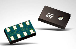
 Pressure Sensor utilizes MEMS technology to detect altitude. Pressure Sensor utilizes MEMS technology to detect altitude.
- Manufacturing the device in this way eliminates wafer-to-wafer bonding and maximizes reliability. The pressure sensor in the LPS001WP is based on a flexible ...
today ThomasNet Industrial News Room (press release) - MEMS technology
MEMS business
- Sensonor Gyro Awarded the Best High Precision MEMS Gyro in the Market
- HORTEN, Norway--(BUSINESS WIRE)--The New Product Innovation Award is a prestigious recognition of Sensonor's accomplishments in the high precision MEMS ...
today Business Wire (press release) - MEMS business
- Emerging MEMS Technologies & Markets – 2010 Report
- Emerging MEMS Technologies & Markets - 2010 Report WHY ANOTHER MEMS MARKET REPORT ? MEMS markets have been and will always be driven by.
marketresearchreports today - MEMS business
- Quiet revolution: MEMS thrives on application diversity
- by Richard Dixon, iSuppli December 2, 2010 - With the exception of the consumer/mobile MEMS market, the high-value MEMS space is the fastest-growing ...
today ElectroIQ - MEMS business
- MEMS : MEMS & Sensors for Smartphones
- MEMS : MEMS & Sensors for Smartphones Report Summary MARKET TRENDS Integration of MEMS components and sensors is not new to the mobile phone.
marketresearchreports today - MEMS business
Nanotechnology
 AcuityXR Technology AcuityXR Technology
- Many nanoscale applications in the semiconductor, medical and precision machining fields today have surface features and defects with dimensions that limit ...
today Photonics.com - Nanotechnology
 Direct writing of sub-5 nm metallic nanostructures Direct writing of sub-5 nm metallic nanostructures
- ... to and interconnects between nanoscale device structures like carbon nanotubes and graphene that have potential uses in electronics applications. ...
today Nanowerk LLC - Nanotechnology
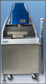
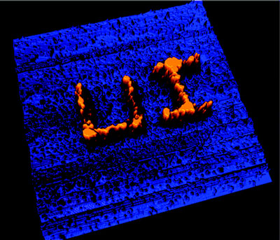
- Bruker Releases New Generation Atomic Force Microscopy at MRS Fall 2010 Meeting
- ... modes and measurement modules that transform Bruker´s AFM systems into turnkey solutions for nanoscale characterization in renewable energy research. ...
today AZoNano.com - Nanotechnology
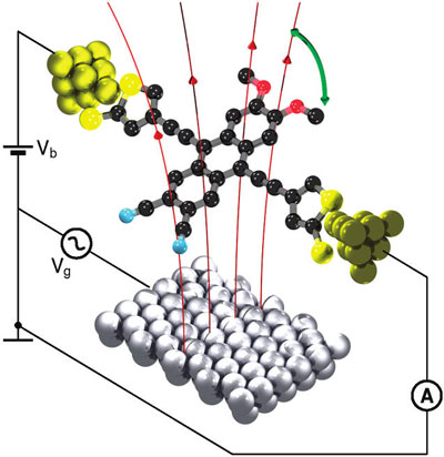
 An electric motor made from a single molecule An electric motor made from a single molecule
- (Nanowerk Spotlight) A fast-growing body of nanotechnology research is dedicated to nanoscale motors and molecular machinery. For the visionary goals of ...
today Nanowerk LLC - Nanotechnology
Featured Process
 MNX offers commercial e-beam lithography services using a state-of-the-art Vistec EBPG 5000+ direct-write tool. This affordable service provides you with the best performance and fastest turnaround times in the industry. | - 50MHz scan speed
- Spot size below 2.5 nm
- Large scan field size
- Fast cycle times
|
Event Calendar
|
|