|
View Mailing Online
MEMS technology
- Packaging Roadmaps at MEPTEC
- 3D will appear first through silicon interposers with through wafer connections and then through chips fabricated with internal TSV for through wafer connections. Bill updated attendees with where the packaging roadmap would be increasing and expanding ...
yesterday ElectroIQ - MEMS technology
- Micro Electro-Mechanical Systems MEMS – Measurement of Surface Features and ...
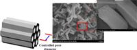
- By AZoNano Editors Microelectro-mechanical systems are being utilized for a variety of applications such as microfluidic pumps, micromirror display devices, and acceleration and pressure sensors. The MEMS units extend the fabrication techniques ...
2011-04-07 AZoNano.com - MEMS technology
- Wet-process technologies for scalable through-silicon vias
- The default scenario for TSV fabrication leverages expensive vacuum-based, dry-process equipment and consumables, such as PE-CVD, iPVD, and ALD, which were originally designed for dual-damascene applications. This has put a tight limitation on TSVs' ...
yesterday ElectroIQ - MEMS technology
Nanotechnology
 Nano pores help boost enzymatic activity Nano pores help boost enzymatic activity
- Rensselaer researchers confined lysozyme and other enzymes inside carefully engineered nanoscale holes. Instead of denaturing, these embedded enzymes mostly retained their 3-D structure and exhibited a significant increase in activity. ...
today domain-B - Nanotechnology
- Nanotechnology Uses Chemical Treatment to Detect Unseen Fingerprints
- By Cameron Chai Hidden fingerprints can be made visible with chemical treatments aimed at molecules that are residual in fingerprints, like those in hair follicle secretions. Xanthe Spindlerm who led a team of researchers at the University of ...
yesterday AZoNano.com - Nanotechnology
Nanotech business
- EU project to develop nanotechnology-based systems for cancer management
- A multidisciplinary SaveMe project has been launched by the European Union (EU) to develop new nanotechnology-based systems for detection, diagnosis and therapy for cancer. One of the most relevant aspects of the study will be the validation of ...
2011-04-07 Health Imaging & IT - Nanotech business
- Regional hubs seen as driver for NY economic growth
- Photos by Hans Pennink/Gannett News Service Alain E. Kaloyeros, senior vice president and chief executive officer for CNSE, holds a 300 mm wafer disk at the College of Nanoscale Science and Engineering, University at Albany, while talking about the ...
2011-04-07 Poughkeepsie Journal - Nanotech business
Featured Process
MNX offers commercial e-beam lithography services using a state-of-the-art Vistec EBPG 5000+ direct-write tool. This affordable service provides you with the best performance and fastest turnaround times in the industry. | - 50MHz scan speed
- Spot size below 2.5 nm
- Large scan field size
- Fast cycle times
|
Event Calendar
- MEPTEC 9th Annual MEMS Symposium
- 2011-05-19
Wyndham San Jose, CA
MEMS - Driving Innovation. Existing Technologies Enable Future Innovations
Visit MNX at this event.
|
|
- EIPBN 2011 ("3-Beams")
- 2011-05-31 - 2011-06-03
Las Vegas NV
World's Leading Symposium on Lithography and Nanofabrication
Visit MNX at this event.
|
|
- Transducers' 11
- 2011-06-05 - 2011-06-09
Beijing, China
The 16th International Conference on Solid-State Sensors, Actuators and Microsystems
|
|
- Sensors Expo & Conference 2011
- 2011-06-07 - 2011-06-08
Rosemont, IL
Focused on sensors and sensor integrated systems, providing over 25 years of technical innovation and thought leadership.
Visit MNX at Booth 208.
|
|
- Microtech Conference & Expo 2011
- 2011-06-13 - 2011-06-16
Boston MA
Uniting innovators to bring microtechnology from laboratory to marketplace
|
|
- COMS 2011
- 2011-08-28 - 2011-08-31
Greensboro NC
Commercialization of Micro - Nano Systems
Visit MNX at this event.
|
|
- MEMS Executive Congress 2011
- 2011-11-02 - 2011-11-03
Monterey, CA
Connecting the MEMS supply chain with MEMS end-users
Visit MNX at this event.
|
|
|
|